Definition and Significance
Micro and nano-scale welding refers to the process of joining or bonding materials at extremely small dimensions, typically in the range of micrometers (μm) to nanometers (nm). It involves the fusion of materials at a microscopic or nanoscopic level to create strong and reliable bonds. This type of welding is crucial in various fields where precise and miniature assemblies are required.
The significance of micro and nano-scale welding lies in its ability to facilitate the fabrication and assembly of intricate and delicate structures. It enables the manufacturing of microelectromechanical systems (MEMS), nanoelectromechanical systems (NEMS), microfluidic devices, biomedical implants, integrated circuits, sensors, and other miniaturized components. Micro and nano-scale welding techniques play a pivotal role in advancing technology and enabling the development of smaller, more efficient, and highly integrated devices.

Applications and Industries
Micro and nano-scale welding techniques find applications in a wide range of industries, including:
- Electronics and Semiconductor Industry: Microscale welding is used in the production of microchips, semiconductor devices, and electronic components. It allows for the precise bonding of tiny wires, leads, and connectors in integrated circuits.
- Biomedical and Pharmaceutical Industry: Microscale welding is employed in the fabrication of medical devices, such as pacemakers, implantable sensors, and drug delivery systems. It enables the assembly of miniature components used in diagnostic tools and surgical instruments.
- Aerospace and Defense Industry: Micro and nano-scale welding is crucial for manufacturing small and lightweight components used in aerospace and defense applications. It enables the assembly of miniaturized sensors, actuators, and electronic systems.
- Optics and Photonics Industry: Micro and nano-scale welding plays a vital role in the fabrication of optical devices, such as fiber-optic connectors, micro-lenses, and photonic integrated circuits. It ensures precise alignment and bonding of optical components.
- Microfluidics and Lab-on-a-Chip Industry: Microscale welding techniques are used in the production of microfluidic devices and lab-on-a-chip systems. They enable the assembly of microchannels, valves, and sensors for manipulating small volumes of fluids.

Challenges and Requirements
Micro and nano-scale welding pose unique challenges due to the reduced size and increased precision required. Some of the challenges and requirements include:
- Heat Management: Welding at the micro and nano-scale generates a small heat-affected zone. Controlling and dissipating heat effectively is crucial to prevent thermal damage to delicate components and nearby materials.
- Precision Positioning and Alignment: Achieving accurate positioning and alignment of the materials to be welded is critical. Sub-micron level precision is often necessary to ensure proper bonding and functionality.
- Material Compatibility: Different materials have varying properties and behaviors at the micro and nano-scale. Welding techniques must be compatible with a wide range of materials, including metals, semiconductors, polymers, and biological substances.
- Process Automation and Control: Assemblies at the micro and nano-scale often involve a large number of repetitive operations. Automation and precise control of welding processes are necessary to ensure consistency and efficiency.
- Equipment and Tooling: Specialized equipment and tools are required for micro and nano-scale welding. These include precision welding systems, microscopes, lasers, electron beams, and focused ion beams, among others.
Micro-scale Welding Techniques
Resistance Spot Welding
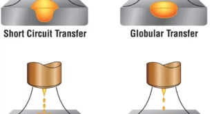
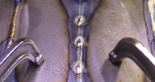
- Principle and Process Resistance spot welding (RSW) is a micro-scale welding technique that involves the localized application of heat and pressure to join materials together. The process utilizes the resistance of the materials to an electric current to generate heat at the interface, causing them to melt and form a bond. Two electrodes are used to apply pressure and deliver the current to the spot where welding occurs.
- Equipment and Materials a. Power supply: RSW requires a power supply capable of delivering high currents for a short duration. b. Electrodes: Copper or other conductive materials are commonly used as electrodes. They provide electrical contact and apply pressure to the welding spot. c. Workpieces: Metals or conductive materials, such as steel, aluminum, or copper, are commonly joined using resistance spot welding.
- Advantages and Limitations
Advantages:
- High-speed welding process
- Minimal distortion and heat-affected zone
- Suitable for high-volume production
- Provides strong and reliable joints
Limitations:
- Limited to metals and conductive materials
- Requires access to both sides of the joint
- Limited control over heat distribution
- Not suitable for very thin or dissimilar materials
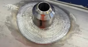
Laser Micro Welding
- Principle and Process Laser micro welding utilizes a focused laser beam to generate localized heat and melt the materials at the welding spot. The laser beam provides precise energy control, allowing for highly controlled and accurate welding. The melted materials solidify, forming a bond.
- Types of Laser Sources a. Nd:YAG (neodymium-doped yttrium aluminum garnet) laser: It emits infrared laser radiation and is suitable for welding metals and some thermoplastics. b. Fiber laser: It produces high-power laser beams with excellent beam quality, making it suitable for welding metals and highly reflective materials. c. CO2 laser: This type of laser emits a continuous wave of infrared radiation and is primarily used for welding non-metallic materials like plastics.
- Advantages and Limitations
Advantages:
- High precision and control
- Minimal heat-affected zone and distortion
- Suitable for a wide range of materials, including metals, plastics, and ceramics
- Capable of welding dissimilar materials
Limitations:
- Equipment and maintenance costs can be high
- Limited access to deep and narrow joints
- Relatively slower process compared to other micro welding techniques
- Sensitive to surface conditions and contaminants
Micro TIG Welding
- Principle and Process Micro TIG (Tungsten Inert Gas) welding, also known as GTAW (Gas Tungsten Arc Welding), employs a non-consumable tungsten electrode and an inert gas shield to protect the welding zone from atmospheric contamination. The electric arc is formed between the electrode and the workpiece, generating the heat required to melt the materials. The melted materials fuse together, creating a bond.
- Equipment and Materials a. Power supply: Micro TIG welding requires a power supply capable of delivering a stable arc and precise control over welding parameters. b. Tungsten electrode: The non-consumable tungsten electrode provides the heat source and electrical contact. c. Shielding gas: Inert gases like argon or helium are used to create a protective atmosphere around the welding area.
- Advantages and Limitations
Advantages:
- Precise control over heat and current
- Suitable for small and intricate welds
- Can be used for a wide range of metals and alloys
- Provides high-quality and aesthetically pleasing welds
Limitations:
- Limited penetration depth compared to other techniques
- Requires skilled operators for precise control
- Limited to accessible joint locations
- Slower process compared to some other micro welding techniques
Micro Plasma Arc Welding
- Principle and Process: Micro plasma arc welding utilizes a focused and high-energy plasma arc to create localized heat for welding. The process involves the ionization of a gas, typically argon or argon-hydrogen mixture, to create a plasma arc. The intense heat of the plasma melts the materials at the welding spot, and upon solidification, a bond is formed.
- Equipment and Materials: a. Power supply: Micro plasma arc welding requires a power supply capable of generating and controlling the plasma arc. b. Torch or nozzle: A specialized torch or nozzle is used to focus the plasma arc and direct it to the welding spot. c. Shielding gas: An inert gas is used to shield the welding area and prevent atmospheric contamination.
- Advantages and Limitations:
Advantages:
- High energy density for deep penetration welds
- Suitable for a wide range of materials, including metals and alloys
- Capable of welding dissimilar materials
- Provides high-quality and strong welds
Limitations:
- Complex equipment setup and maintenance
- Limited to accessible joint locations
- Limited control over heat distribution
- Sensitivity to surface conditions and contaminants
Nano-scale Welding Techniques
Electron Beam Welding
- Principle and Process Electron beam welding (EBW) is a nano-scale welding technique that utilizes a focused beam of high-energy electrons to generate localized heat for welding. The process involves directing the electron beam onto the welding spot, causing the materials to melt and form a bond. As the melted materials solidify, a strong and precise weld is created.
- Equipment and Materials a. Electron beam gun: It generates the high-energy electron beam and controls its focus and intensity. b. Vacuum chamber: EBW requires a vacuum environment to prevent the scattering and absorption of electrons. c. Workpieces: Metals and conductive materials, including alloys, are commonly joined using electron beam welding.
- Advantages and Limitations
Advantages:
- Excellent precision and control over heat input
- Deep penetration capability
- Minimal heat-affected zone and distortion
- Suitable for a wide range of materials, including refractory metals
Limitations:
- Requires a vacuum environment
- Expensive equipment and maintenance
- Limited access to complex geometries
- Sensitive to surface contamination and impurities
Focused Ion Beam Welding
- Principle and Process Focused ion beam (FIB) welding is a nano-scale welding technique that employs a focused beam of ions to create localized heat for welding. The process involves directing the ion beam onto the welding spot, causing the materials to melt and fuse together. FIB welding is often used for precise and small-scale modifications and repairs.
- Equipment and Materials a. Ion beam source: It generates and focuses the beam of ions, typically gallium ions. b. Vacuum chamber: FIB welding requires a vacuum environment to prevent scattering and interactions with atmospheric gases. c. Workpieces: FIB welding is suitable for a wide range of conductive materials, including metals and alloys.
- Advantages and Limitations
Advantages:
- Precise control and accuracy
- Capable of welding at the nanoscale
- Allows for modifications and repairs on small features
- Suitable for a variety of materials
Limitations:
- Limited penetration depth
- Relatively slower process compared to other techniques
- Expensive equipment and maintenance
- Limited access to complex geometries
Nanoparticle Welding
- Principle and Process Nanoparticle welding involves the use of nanoparticles as a heat source to induce localized melting and bonding of materials. The process typically involves depositing or applying nanoparticles onto the welding spot and applying an external stimulus, such as heat, pressure, or electromagnetic fields, to initiate the welding process. The nanoparticles act as a heat source, promoting the fusion of materials and creating a bond.
- Types of Nanoparticles Used a. Metal nanoparticles: Metal nanoparticles, such as gold, silver, or platinum, are commonly used for nanoparticle welding due to their high thermal conductivity and stability. b. Nanocomposite particles: Composite nanoparticles, containing a mixture of materials, can be used to tailor the welding process and enhance the properties of the joint.
- Advantages and Limitations
Advantages:
- Precise control over heat input and localization
- Can be used for joining dissimilar materials
- Versatile and adaptable to different welding scenarios
- Potential for integration with other manufacturing processes
Limitations:
- Optimization of nanoparticle composition and size is critical
- Limited to materials compatible with nanoparticle deposition methods
- May require additional processing steps for nanoparticle removal
- Limited to certain joint configurations and geometries
Materials and Substrates for Micro and Nano-scale Welding
Metals and Alloys Metals and alloys are commonly used materials in micro and nano-scale welding due to their conductivity, strength, and versatility. Various metals and alloys can be welded using different welding techniques, including resistance spot welding, laser micro welding, micro TIG welding, and electron beam welding. Examples of metals and alloys used in micro and nano-scale welding include stainless steel, aluminum, copper, titanium, nickel, and their respective alloys. These materials find applications in industries such as electronics, aerospace, automotive, and medical devices.
Semiconductors Semiconductors play a crucial role in modern electronic devices, and their welding is essential for the fabrication of integrated circuits, microchips, and other electronic components. The most common semiconductor materials, such as silicon (Si), germanium (Ge), and III-V compound semiconductors like gallium arsenide (GaAs) and indium phosphide (InP), require specialized welding techniques. Laser micro welding and micro TIG welding are often employed for joining semiconductors. Welding of semiconductors requires careful control of heat input to prevent damage to delicate structures and maintain electrical properties.
Polymers Polymers, or plastics, are widely used in various industries, including electronics, automotive, and medical devices. Micro and nano-scale welding of polymers allows for the fabrication of microfluidic devices, lab-on-a-chip systems, and miniature components. Techniques such as laser welding, ultrasonic welding, and nanoparticle welding are utilized for joining polymers. Polymeric materials such as polycarbonate (PC), polypropylene (PP), polyethylene (PE), and polydimethylsiloxane (PDMS) are commonly welded at the micro and nano-scale. Welding of polymers requires precise control of heat and pressure to avoid degradation or warping of the material.
Biological Materials Welding techniques are also used for joining biological materials in applications such as medical devices, tissue engineering, and biofabrication. Biological materials include biomaterials, tissues, cells, and bioresorbable polymers. Laser welding and nanoparticle welding are commonly employed for joining biological materials due to their non-contact nature and precise control over heat input. Welding of biological materials requires special considerations, including compatibility with living systems, minimizing thermal damage to sensitive biological structures, and ensuring biocompatibility and sterility.
Challenges and Future Directions
Heat Control and Thermal Management One of the critical challenges in micro and nano-scale welding is precise heat control and thermal management. The small size of the weld area makes it susceptible to rapid heat transfer and localized thermal effects. Future advancements should focus on developing improved heat control techniques, such as optimized power delivery, enhanced cooling methods, and advanced heat management systems, to ensure minimal heat-affected zones, reduce distortion, and maintain material properties.
Precise Positioning and Alignment Achieving precise positioning and alignment of the welding components is crucial for successful micro and nano-scale welding. As the size of the welds decreases, the accuracy requirements become more stringent. Future directions should involve the development of advanced positioning systems, robotic automation, and in-situ monitoring techniques to ensure accurate alignment of the welding components, even in complex geometries and confined spaces.
Process Automation and Control The automation and control of micro and nano-scale welding processes are essential for achieving consistent and reliable results. Future developments should focus on the integration of advanced sensors, real-time monitoring systems, and feedback control mechanisms to enable automated adjustments during the welding process. This will enhance process repeatability, reduce human errors, and improve the overall efficiency and productivity of micro and nano-scale welding operations.
Integration with Other Manufacturing Techniques Micro and nano-scale welding techniques need to be seamlessly integrated with other manufacturing techniques to enable complex and multifunctional microfabrication processes. This integration can involve combining welding with additive manufacturing, micro-machining, or surface modification techniques. Future directions should explore hybrid manufacturing approaches, where micro and nano-scale welding is synergistically combined with other techniques, enabling the fabrication of intricate structures and functional devices.
Emerging Applications and Research Areas The field of micro and nano-scale welding continues to expand, leading to emerging applications and research areas. Some of the future directions include:
- Biomedical Applications: Advancements in micro and nano-scale welding techniques can contribute to the development of bioresorbable implants, tissue engineering scaffolds, and drug delivery systems.
- Nanomaterials and Nanodevices: Welding techniques can be utilized for the fabrication of nanoscale structures, such as nanowires, nanotubes, and nanosensors, enabling advancements in electronics, energy storage, and sensing applications.
- Microelectronics and Photonics: Micro and nano-scale welding plays a vital role in the assembly of microelectronic components, integrated circuits, and photonic devices. Future research can focus on enhancing welding techniques for high-density interconnections, miniaturized optoelectronic devices, and flexible electronics.
- Microfluidics and Lab-on-a-Chip Systems: Welding techniques are essential for the fabrication of microfluidic devices and lab-on-a-chip systems, enabling advancements in chemical analysis, point-of-care diagnostics, and biomedical research.
FAQs
What is nano welding?
Nano welding refers to the process of joining materials at the nanoscale, typically involving the use of specialized techniques and equipment to create precise and controlled bonds between nano-sized components or structures.
What is difference between nano and micro?
The main difference between nano and micro is the scale at which they operate. Nano refers to the nanometer scale, which is one billionth of a meter, while micro refers to the micrometer scale, which is one millionth of a meter. Nano is smaller than micro in terms of size.
What is the scale of micro and nano?
The scale of micro typically ranges from a few micrometers (µm) to a few hundred micrometers, whereas the scale of nano ranges from a few nanometers (nm) to a few hundred nanometers.
What is the difference between nanoscale and macroscale?
The difference between nanoscale and macroscale lies in the size of the objects or structures being observed or manipulated. Nanoscale refers to the realm of objects or phenomena on a very small scale, typically at the nanometer level, while macroscale refers to the larger-scale objects or phenomena that are visible to the naked eye.
What is micro welding?
Micro welding is the process of joining materials at the microscale, typically involving small components or structures. It requires precise control of heat and parameters to create strong and reliable bonds between the materials.
What are micro welding techniques?
Micro welding techniques include resistance spot welding, laser micro welding, micro TIG welding, micro plasma arc welding, and electron beam welding. These techniques are specifically designed to operate at the microscale, offering precise control and accuracy.
What is micro and macro scale?
Micro and macro scale refer to different size ranges. Micro scale typically ranges from a few micrometers to a few hundred micrometers, while macro scale refers to the larger-scale objects or phenomena visible to the naked eye.
What is the difference between micro and macro and nano?
The main difference between micro, macro, and nano lies in their size scales. Micro refers to the micrometer scale, macro refers to the larger-scale visible objects, and nano refers to the nanometer scale, which is smaller than micro.
What is between micro and macro scale?
Between micro and macro scale, there is the mesoscale, which bridges the gap between the two. The mesoscale refers to the size range between micro and macro, typically ranging from a few hundred micrometers to a few millimeters.
Why is it called nano?
Conclusion
Micro and nano-scale welding techniques encompass a range of processes that enable the precise joining of materials at small scales. This outline has explored various welding techniques, including resistance spot welding, laser micro welding, micro TIG welding, micro plasma arc welding, electron beam welding, focused ion beam welding, and nanoparticle welding. It has also discussed the materials and substrates commonly used in micro and nano-scale welding, such as metals and alloys, semiconductors, polymers, and biological materials. Furthermore, the outline has highlighted the challenges and future directions in the field, including heat control, precise positioning, process automation, integration with other manufacturing techniques, and emerging applications.
Micro and nano-scale welding plays a crucial role in various industries and research fields. It enables the fabrication of miniature components, microelectronic devices, integrated circuits, and microfluidic systems. The ability to join materials at such small scales allows for the development of advanced technologies with improved performance, miniaturization, and integration. Micro and nano-scale welding also enables advancements in areas such as electronics, aerospace, automotive, medical devices, biotechnology, and nanotechnology.
The field of micro and nano-scale welding holds significant potential for further advancements. Ongoing research and development efforts are focused on addressing challenges related to heat control, precision, automation, and integration. As these challenges are overcome, the impact on industries will be substantial. Micro and nano-scale welding techniques will enable the fabrication of highly efficient and miniaturized devices, advancements in biomedical applications, the development of novel nanomaterials and nanodevices, and the realization of complex microfabrication processes. These advancements will drive innovation, enhance product performance, and open up new possibilities in various industries, ranging from electronics and healthcare to energy and manufacturing.